![You suck at protoshop. No, you [i]really[/i] oo.](http://blog.gg8.se/images/you-suck-at-photoshop-you-really-do-your-awful.png)


Gameboy project week 8: The white Nintendo Power official flash cartridge, a tale of reverse engineering, sweat and tears
February 25th, 2013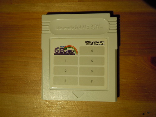
This week’s project concerns this cartridge, the official Nintendo Power flash cartridge. It used to actually be sold by Nintendo for 2500 yen and you could by games from a special kiosk starting at 800 yen at the Lawson department store. (About US$27 and US$9 respectively at today’s exchange rate.) The kiosks are long gone, but the cartridges remain in the wild. (However one page in Japanese from the time remains. It mentions how the launch is delayed because of the earthquake in Taiwan, the massive 921 earthquake)
Since these are flash cartridges they are in theory writeable, which would make them useful for, for example Little Sound Dj or other homebrew software. However, writing to them has proven difficult. The currently only known way of writing to them is with a software called FMGBx by Mootan. The program works but requires flasher hardware that is difficult to get and and in all cases are using an LPT port interface. Options include Bungs GB Xchange, a modified GBA flasher and two homebrew solutions using discrete 74hc logic. Clearly, there’s room for improvement.
My story with this cartridge started a couple of years back, when Nullsleep, aka Jeremiah sent me one for free, for the purpose of figuring out the protocol. At the time, I did not have access to an easily programmable flasher (more on that later) so my best way of trying to interface this cartridge was with a cartridge swap technique. I would write a special program which I would burn to some other cartridge. Said program would copy itself to the Gameboy’s internal RAM. I would then remove the source cartridge and insert the target cartridge, in this case the Nintendo Power cartridge. This method was unstable. The Gameboy would often crash or otherwise misbehave.
Flash chips typically communicate through a protocol where you give it commands by writing standard sequences. One such common sequence is: $AA to address $5555, $55 to address $2AAA, $90 to address $5555, which enter silicon ID mode. In this mode, you can detect the manufacturer and chip model. Other commands include, program, erase and, depending on the manufacturer and model, memory sector protection. I tried different versions of these commands, to no avail. I soon gave up with finding the secret to the Nintendo Power cartridge.
Fast forward a couple of years, I once again regained my interest in this cartridge, and one thing I tried in order to find clues about how to flash it, was to look at the Nintendo Power menu program that came with the cartridge. I did not find any clues on how to access the flash, but I did find a little secret. If you press all button simultaneously, you get to a debug screen, which performs a couple of self tests on the cartridge.
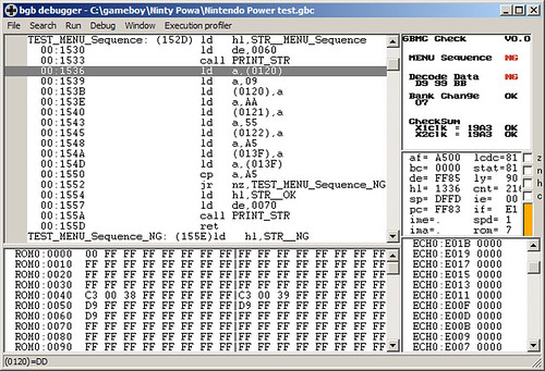
Clearly you cannot hold all eight buttons (including all four directions on the D pad) simultaneously, so this must be a feature designed for a special device with all the buttons hardwired to be pressed in order to boot into this test. The jump takes place at position 017D, and if you want to make the ROM always boot the test, you can change bytes 017D and 017E to 00. The screenshot shows a further modified version of the ROM which does not stop if one single test fails.
The tests “bank change” and “checksum” are straightforward. Bank change checks basic MBC type functionality. Checksum calculates the ROM checksum in GBC single and double speed mode. Presumably it would fail if the flash chip has a too low speed grading for the GBC double speed mode.
The menu sequence and decode data are more interesting. They write to and read from a number of memory positions in the 0120-013F memory range. These are clearly IO registers of some sort, which are inconspicuously placed in the area that is otherwise used for the cartridge header. I knew this was significant, but didn’t really know how to use it to write to flash.
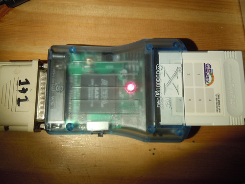
Fast forward some more to this week. I now finally have a Bung GB Xchanger, which I can connect to my rusty old LPT laptop. I can confirm that I can indeed use this FMGBx plus the Xchanger to write ROMs to the cartridge. I wrote a ROM to the cartridge, that I created, which allows code to be downloaded over the link cable. I’m using this together with the Nanoloop adapter for a quick development cycles so I can do experiments easily.
Now comes the difficult part. I can either write blindly to the cartridge and hope to find something interesting, or I can reverse engineer this software. Well, I don’t care, let’s reverse engineer it. Let’s find out from the inside how this works. This is the process that took hours and a lot of frustration. Even though IDA (a nice disassembler) does a very good job at disassembling and organizing the code flow visually, you still need to find what you’re looking, which can be like finding a needle in a haystack. Even though it may seem easy when condensed to a text like this, it can be painstaking.
So after a while, I did find the function that writes to the LPT port. Check xrefs. Find various functions calling it. Find various functions calling that. Get tired and go make some food. Get back and lose my train of thought from before. Make a hypothesis about which code path is for the NP cartridge. Test hypothesis on the Gameboy and find it to be incorrect. Have doubts about the exact format of the LPT write function.
Decide to create a “detour” DLL which is injected to the process and hooks all IO accesses and logs them to a file. Struggle with this while learning. Transfer the DLL to the LPT lappy. Program crashes because of badly formatted DLL code. Rinse and repeat. Fix the error and copy the DLL to the laptop yet another time. Be unsure for a bit more, how exactly the logged data is formatted. Spend some time trying to correlate the log data to the disassembled machine code. Form a couple of hypotheses on what exactly the code does and try them on the Gameboy. Still nothing.
Have a heureka moment about what the code does. The code has two functions, one to set the target “action” (latch the lower and upper address byte, or data byte) and one function to perform the chosen action. These usually come in pairs, as such:
push    0                            ; \ Set mode
call    _write_port_status           ; /

push    0AAh                         ; \ Latch lower address byte
call    _write_port_data             ; /

push    1                            ; \ Set mode
call    _write_port_status	     ; /

push    2Ah			     ; \ Latch upper address byte
call    _write_port_data	     ; /

push    2			     ; \ Set mode
call    _write_port_status	     ; /

push    83h			     ; \ Latch data byte
call    _write_port_data	     ; /

push    3			     ; \ Set mode
call    _write_port_status	     ; /
(_write_port_data and _write_port_status are my names given to these functions to more easily remember what they do. Originally, they would just be named by their memory address.)
This would for example write the value $83 to the address $2AAA, as part of some flash command.
However, what threw me off near the end of this process was that in some places, there multiple _write_port_data statements, which I assumed meant repeat a write to the same address. So, I had annotated the flash access unlock sequence (to be able to access the flash at all) as:
[0120]=09
[0120]=aa
[0120]=55
[013f]=a5
The three supposed writes to 0120 were done with such repeated _write_port_data calls. However, those repeated calls had an automatic increment of the address, so the actual addresses were 0120, 0121 and 0122. I realized this when looking back for a second at the menu ROM disassembly in BGB shown above. And this was actually the last hurdle before I could successfully do a silicon ID command to the flash chip and get back that the manufacturer ID is $C2 (Which means Macronix, just like it says on the chip) and the device ID is $89.
In other words, the Nintendo Power cartridge is officially unlocked. In the future, I will come up with some more user-friendly way of flashing these cartridges, but this week’s project ends here. Here’s a cathartic proof of concept: a program that is loaded from the computer over the link cable (this has been my development setup for probing the cartridge) and prints some information about the cartridge, and then erases the cartridge. When rebooting the cartridge, the logo is empty, which shows that it hs been erased.
Btw, if you look inside the cartridge, you can see that the RAM chip, UT621024, is clearly a 128 kiB chip, but apparently LSDj can only access half of that. I can probably fix that in LittleFM so the full 128 kiB can be used.
Appendix: Command sequences:
Enable flash chip access:
(With only this command, you can do silicon ID command, but not erase/program.)
[0120]=09
[0121]=aa
[0122]=55
[013f]=a5

Disable flash chip protection: (Enables erase/program. Probably flips the /WP pin.)
[0120]=0a
[0125]=62
[0126]=04
[013f]=a5
[0120]=01
[013f]=a5
[0120]=02
[013f]=a5

Perform one write to flash chip memory space:
(Using this, you can give flash commands to the chip.)
[0120]=02
[0120]=0f
[0125]=HH        ;Upper address byte
[0126]=LL        ; Lower address byte
[0127]=DD        ; Data
[013f]=a5        ; Perform the action
(Sorry. This week’s project comes without a ROM.)
February 25th, 2013 at 6:42 am
Great trial and error work. Tedious troubleshooting does not always pay off unless you have the patience to work through problems. You seem to be able to do that very well.
April 11th, 2013 at 4:12 pm
I have one of these cartridges, how much do you think it is worth nowadays?
August 23rd, 2013 at 2:22 am
Were you able to register the software Flashman GBx?
I have emailed Mootan, but have not heard from him. I’m doing as you say above. I was able to acquire a GBX transferer, so now I just need to register my software. Thank you for any help.
Chris
September 1st, 2013 at 3:26 pm
There’s one of these on ebay atm for £20, tempted to buy it…but it looks like it’ll be a lot of work to get it working lol
September 12th, 2013 at 6:19 am
can’t understand neraly anything about programming, but i readed all the history and i loved it.
September 13th, 2013 at 11:55 am
[...] Proyecto para intentar reutilizar este cartucho. [...]
October 3rd, 2013 at 5:38 am
Wow, nice work. So you got the information about pressing all the keys together by looking into the code of the Nintendo Power menu program?
October 3rd, 2013 at 12:42 pm
Yeah. I was single stepping through the program from the beginning and noticed that weird button check.
December 19th, 2013 at 10:40 am
Great job! But it’s so difficult.
October 22nd, 2015 at 10:52 am
Can you share the flash instruction to get the device ID?