![You suck at protoshop. No, you [i]really[/i] oo.](http://blog.gg8.se/images/you-suck-at-photoshop-you-really-do-your-awful.png)


PCB Manufacturing at my university (Pictures)
December 19th, 2008So I etched a PCB at my university today, and i thought I’d share some pictures. Today’s PCB is an XR-2206 Based Voltage Controlled Oscillator, a rad oscillator synth module.
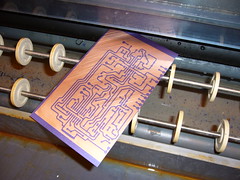
The manufacturing process involves several transfers: Paper -> Photographic film -> Photoresist -> Copper. Let’s begin with a picture of three of the steps, the printed paper, the film and the finished PCB.
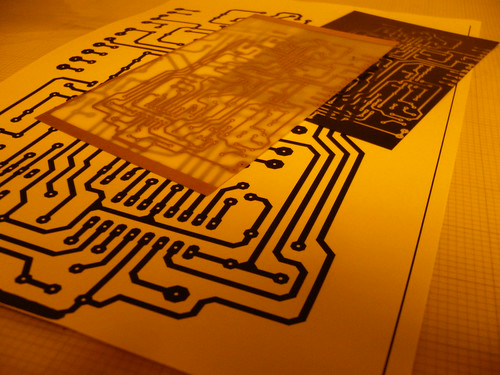
So the first thing I have to do is print the layout on paper. It needs to be printed with high contrast and dense blackness to transfer well to the photographic film. For this PCB I chose to do the transfer double sized to increase the contrast, but you can transfer it with a 1:1 size source printout. (Or anything between)
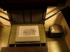
 The next step is to expose the photographic film. This is done with a device consisting of a glass plate under which you put the original, and a lid under which you put the film. Both the glass and the lid have vacuum suction to keep the paper and film in place.
When you press a button, two light sources are turned on to expose the film. The light is reflected against the source material through a lens, and onto the film. The film is, as far as I know standard black and white photographic film. In other words, this device is a giant camera.
The next step is to develop the film. This is done by putting the film first in a “developer” fluid to make the image visible, and then in a “fixer” fluid to protect the film from light. Until the film has been completely developed, the photo room must be lit strictly using a faint red light to avoid exposing the film by accident.

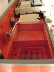
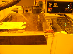 Next up is transferring the image on the film to the photoresist on the board. Unfortunately I forgot to take a picture of this step, but it’s done by exposing the photoresist to UV light through the film. The photoresist will be weakened in all areas exposed to the UV light. The weakened areas will then be etched away using a CaCO3 (Calcium carbonate) solution in the first etching machine. The result is that the copper is exposed at those parts. (Left picture) And then I put it through the second etching machine, containing iron chloride, which will etch away the exposed copper areas. (Right picture)

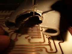
Almost done. The last step is to put the board into a stripper fluid (NaOH, Sodium hydroxide) to remove the remaining photoresist.
After drilling the holes the PCB is ready to be equipped with components.
April 15th, 2013 at 8:35 pm
Hi I am Baker from Jordan
well your steps is normal , the same I do but if you tell me
why you use CaCo3 befor etching
and why you use Iron chloride instead of ferric chloride ?
is it stronger ?
I do not use calcuim carbonate ..is it necessary for good result?
April 15th, 2013 at 8:56 pm
Hello. This depends on which method you use. This method is using a protective layer (photoresist) which is hardened by light. This is done with UV light. When you apply CaCO3, the part of this layer that is soft will be removed, but the part of the layer that is hard will stay.
If you are using a different method, you need a different chemical than CaCO3. CaCO3 is only for the photoresist method.
Iron chloiride is the same as ferric chloride. Different names.
March 26th, 2019 at 8:27 am
[...] See also GameBoy genius’s page PCB Manufacturing at my university (Pictures) [...]